7 Ways Your MCU Can Talk to FPGA : On Shrike

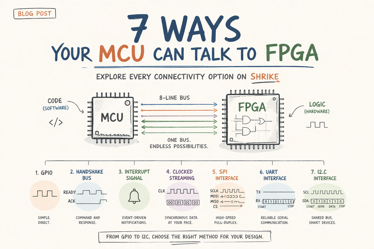
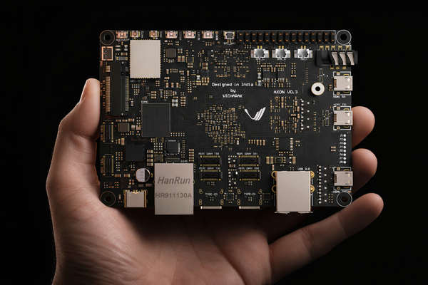
When you first look at the Shrike board, you see two chips — a microcontroller and an FPGA. What you don't immediately see is the 8-line bus that connects them on the PCB. This bus is, in many ways, the most important part of the board. Without it, you just have two independent chips sitting on a single PCB. With it, you have a co-processing system.
In this log, we'll explore every way you can use this bus — from the simplest GPIO toggle all the way to full hardware SPI, UART, and I2C communication. By the end, you'll understand not just how to use each method, but when and why you'd pick one over another.
Before we begin, let me tell you what this blog is not about:
- How to flash a bitstream to the FPGA (see the Getting Started guide for that)
- How to set up the toolchain or write your first Verilog
- Or anything about the FPGA's internal architecture (see the architecture log for that)
This is purely about the link between the two chips — the bridge between MCU and FPGA on the Shrike board.
The Bus: What's Actually There
Every Shrike board connects its host MCU to the SLG47910 ForgeFPGA through an 8-bit bus routed on the PCB. But not all 8 lines are equal.
2 lines are control signals — EN (enable) and PWR (power). These exist to reset and initialize the FPGA. You don't use them for data.
4 lines are dual-purpose — they serve as the SPI configuration bus during FPGA programming, and then become general-purpose IO after the bitstream is loaded. This is important to internalize:
The same 4 wires that program the FPGA become your data channel at runtime.
2 lines are pure GPIO — FPGA pins 17 and 18, connected directly to MCU GPIOs and also routed to the IO header. These are configurable via a 0Ω resistor on the PCB.
Check the schematics for more details.
Here's the complete map for Shrike-Lite and Shrike:
| FPGA Pin | Function | MCU GPIO | MCU Alternate Function |
|---|---|---|---|
| EN | Enable | GPIO 13 | — |
| PWR | Power control | GPIO 12 | — |
| 3 | SPI_SCLK | GPIO 2 | SPI0 SCK |
| 4 | SPI_SS | GPIO 1 | UART0 RX |
| 5 | SPI_MOSI | GPIO 3 | SPI0 TX |
| 6 | SPI_MISO | GPIO 0 | UART0 TX |
| 18 | GPIO | GPIO 14 | I2C1 SDA |
| 17 | GPIO | GPIO 15 | I2C1 SCL |
Look at the "MCU Alternate Function" column carefully. Those are not coincidences. The pin mapping was designed so that after programming, the SPI pins line up with the MCU's hardware SPI peripheral, the UART pins line up with UART0, and the GPIO pins line up with I2C1. This is what makes Shrike's co-processing story work — you get hardware-accelerated communication for free, just by using the right peripheral.
The Two Phases of the Bus
Phase 1: Programming
When you call shrike.flash("/bitstream.bin") from Shrike library , the 4 dual-purpose pins operate as an SPI bus. The MCU power-cycles the FPGA, clocks out the entire bitstream through MOSI/SCLK, and then pulses EN to activate the design. After this, Shrike Flash releases the bus.
Phase 2: Runtime
Once the bitstream is loaded, those 4 SPI pins no longer behave as SPI — they are whatever your Verilog defines them to be. The FPGA doesn't remember that it was programmed over SPI. It only knows its current configuration.
This is the moment where you choose how the two chips will talk.
Method 1: Simple Parallel IO
The most basic approach. No protocol, no clock, no handshake. Each interconnect pin is an independent signal — the MCU writes a GPIO, the FPGA sees it change. Or the FPGA drives a pin high, and the MCU reads it.
When to use this: Event flags. Status bits. "Is the sensor in range?" — a yes/no answer from the FPGA.
FPGA (Producer)
on every clock:
    if sensor_event_detected:
        event_flag ← 1
    else if timeout_elapsed:
        event_flag ← 0
MCU (Consumer)
loop:
    value ← read_gpio(EVENT_PIN)

    if value == HIGH:
        handle_event()

    wait(small_interval)
Why this works: The FPGA evaluates the sensor every clock cycle — 50 million times per second. The MCU polls at whatever rate it wants. The FPGA never misses the event, and the MCU reads the result when it's ready. This is the core idea behind MCU-FPGA co-processing.
Note : This blog only uses sudo codes or algorithms if you wish to see real implementation please check the shrike repo here.
Method 2: Command / Response
Use 4 pins as a data bus and 2 pins for handshake signals. The MCU places a 4-bit command on the bus and raises a READY flag. The FPGA reads the command, processes it, places a 4-bit response on the bus, and raises an ACK flag.
This is the first protocol that involves both sides taking turns. The data bus changes direction mid-transaction.
MCU_READY  ____╱‾‾‾‾‾‾‾╲____________
DATA[3:0]  ════╳ CMD    ╳════════════
FPGA_ACK   ____________╱‾‾‾‾‾╲______
DATA[3:0]  ════════════╳ RESP ╳═════
MCU
function send_command(cmd):
    set DATA as OUTPUT
    write DATA ← cmd

    set MCU_READY ← HIGH

    wait until FPGA_ACK == HIGH

    set DATA as INPUT
    response ← read DATA

    set MCU_READY ← LOW
    wait until FPGA_ACK == LOW

    return response
FPGA
state ← IDLE

on every clock:
    if state == IDLE:
        if MCU_READY == HIGH:
            cmd ← read DATA
            state ← PROCESS

    if state == PROCESS:
        result ← execute(cmd)
        state ← RESPOND

    if state == RESPOND:
        drive DATA ← result
        set FPGA_ACK ← HIGH

        if MCU_READY == LOW:
            set FPGA_ACK ← LOW
            release DATA bus
            state ← IDLE
The key insight: This pattern is useful when you have multiple FPGA functions and want to select between them at runtime. Send command 0x01 for sensor A, 0x02 for sensor B, 0x03 for status. One interface, multiple capabilities.
Limitation: 4-bit data width. For anything larger than a nibble, you need multiple round-trips. That's where the hardware peripherals come in.
Method 3: Interrupt-Style Notification
Sometimes the FPGA needs to tell the MCU "something happened" without the MCU constantly polling. The FPGA drives a pin high, and the MCU catches it with a hardware interrupt.
FPGA
on event_detected:
    set IRQ_PIN ← HIGH

on event_cleared:
    set IRQ_PIN ← LOW
MCU
interrupt_handler():
    event_flag ← TRUE

main_loop:
    if event_flag == TRUE:
        event_flag ← FALSE
        handle_event()
This is not a communication protocol — it's a notification mechanism. You'll often combine this with another pattern. For example: FPGA raises an interrupt, MCU responds by reading data over SPI.
Method 4: Clocked Streaming
For moving larger amounts of data using GPIO alone — the FPGA generates a clock on one pin, a data-valid signal on another, and streams nibbles on the remaining 4 pins. The MCU samples on each rising edge. This is niche.
FPGA (Streamer)
for each data_nibble in stream:
    write DATA ← data_nibble
    set VALID ← HIGH

    toggle CLK

    wait one cycle

set VALID ← LOW
MCU(Receiver)
loop:
    wait until VALID == HIGH

    on rising edge of CLK:
        nibble ← read DATA
        store(nibble)
You'd use it when you need moderate throughput but can't or don't want to implement a full SPI/UART peripheral in Verilog. For most people, Pattern 5 (SPI) is a better choice.
For all the Method from here , we assumes that you have basic understanding of communication protocol like UART, I2C and SPI. If not they are not rocket science you can easily learn about them from the open internet.
Method 5: SPI Communication
This is where things get serious. We will here assume that you know what SPI is and how it works if not use the open internet to figure it out.
After shrike.flash() completes and releases the SPI bus, those same 4 pins are free. You re-initialize them as a standard SPI peripheral — the MCU becomes the master, and the FPGA runs a Verilog SPI slave.
MCU (SPI Master)                    FPGA (SPI Slave)
 │                                   │
 │  GPIO 2 ──── SCLK ─────────────► │ Pin 3
 │  GPIO 1 ──── CS ────────────────► │ Pin 4
 │  GPIO 3 ──── MOSI ─────────────► │ Pin 5
 │  GPIO 0 ◄─── MISO ──────────────│ Pin 6
The MCU's hardware SPI peripheral handles clocking, buffering, and optionally DMA. You get full 8-bit transfers at MHz speeds — not 4-bit nibbles over bit-banging.
The Verilog SPI slave is a shift register that samples MOSI on the rising edge of SCLK and shifts out MISO on the falling edge. When 8 bits have been clocked in, the byte is latched and a new byte is loaded for the next transfer.
MCU
initialize SPI

function transfer(byte_out):
    set CS ← LOW

    byte_in ← spi_send_and_receive(byte_out)

    set CS ← HIGH

    return byte_in
FPGA (SPI Slave)
on rising edge of SCLK:
    shift_in MOSI into rx_shift_register

on falling edge of SCLK:
    output next bit from tx_shift_register to MISO

if 8 bits received:
    received_byte ← rx_shift_register
    response_byte ← process(received_byte)
    load tx_shift_register ← response_byte
Why SPI is the default choice for serious projects: Full 8-bit data width, hardware peripheral handles timing, DMA-capable on both RP2040 and ESP32-S3, and the pins were literally designed for this. The same wires that programmed the FPGA become your high-speed data channel.
The complete SPI slave Verilog module and firmware are in the example.
Method 6: UART Communication
FPGA pins 4 and 6 map to MCU GPIO 1 (UART0 RX) and GPIO 0 (UART0 TX). After programming, you can run UART between the MCU and a UART core implemented in Verilog.
MCU                                  FPGA
 │  GPIO 0 ──── TX ────────────────► │ Pin 6 (FPGA's RX)
 │  GPIO 1 ◄─── RX ─────────────── │ Pin 4 (FPGA's TX)
UART only uses 2 pins, freeing 4 others for GPIO, SPI, or I2C. The protocol is well-understood, easy to debug (open a serial terminal), and can carry arbitrarily long messages. The tradeoff is speed — UART tops out at a few megabaud.
The Verilog side is modular: separate uart_rx.v and uart_tx.v modules wired together by a top.v that implements your application logic. If you've seen the uart_sum example in the repo, that's exactly this pattern — the FPGA receives two bytes over UART, computes their sum in hardware, and sends the result back.
MCU
initialize UART

function send(data):
    uart_write(data)

function receive():
    wait until uart_data_available()
    return uart_read()
FPGA
UART_RX module:
    on valid frame:
        received_byte ← data
        pass to logic

UART_TX module:
    when data_ready:
        transmit byte serially with start/stop bits

application_logic:
    byte1 ← receive
    byte2 ← receive

    result ← compute(byte1, byte2)

    transmit(result)
When to pick UART over SPI: When you need a simple, bidirectional byte stream and don't want the overhead of chip-select and clock management. UART is also easier to debug — you can literally connect a USB-serial adapter to the FPGA's TX pin and see what it's sending.
The complete UART example with modular Verilog is in this example .
Method 7: I2C Communication
FPGA pins 17 and 18 connect to MCU GPIO 14 and 15 — the I2C1 SDA and SCL lines. The FPGA implements an I2C slave with a 7-bit address, and the MCU talks to it using the standard Wire library.
MCU                                  FPGA
 │  GPIO 14 ──── SDA ◄────────────► │ Pin 18
 │  GPIO 15 ──── SCL ─────────────► │ Pin 17
This one is interesting for a reason beyond just communication. Because these pins are also routed to the IO header, you can have external I2C sensors on the same bus as the FPGA. The MCU addresses the FPGA at (say) 0x42 and a temperature sensor at 0x48 — same two wires, multiple devices.
MCU (Master)
function read_register(addr, reg):
    start_condition()

    send(addr + WRITE)
    send(reg)

    repeated_start()

    send(addr + READ)
    data ← read_byte()

    stop_condition()

    return data
FPGA (Slave)
on START condition:
    capture address

if address matches:
    if WRITE:
        receive register_address
        receive data → store in register_map

    if READ:
        data ← register_map[requested_register]
        transmit(data)

handle ACK/NACK accordingly
The Verilog I2C slave is the most complex of the three — it needs START/STOP detection, address matching, ACK generation, and bidirectional SDA handling. The complete implementation is in the examples .
When to pick I2C: When you want a register-based interface (read register 0x01, write register 0x02) or when you need to share the bus with external sensors. Also useful when you've already used the SPI and UART pins for other things and only have pins 17/18 left.
Choosing the Right Pattern
Here's how I think about it:
- "I just need a yes/no signal from the FPGA" → Pattern 1 (Parallel IO)
- "I need the FPGA to wake up the MCU" → Pattern 3 (Interrupt) + another pattern for data
- "I need to send commands and get responses" → Pattern 6 (UART) for simplicity, Pattern 5 (SPI) for speed
- "I need high-throughput data exchange" → Pattern 5 (SPI)
- "I want a register-based interface or shared bus" → Pattern 7 (I2C)
- "I need maximum flexibility with minimum pins" → Pattern 6 (UART) — only 2 pins.
And you can combine them. A typical advanced project might use SPI for data, one GPIO for interrupt, and one GPIO for a control flag. Or UART for commands and I2C for register access. The 6 data lines plus 2 control lines give you enough room to mix and match.
| Protocol | Pins | Data Width | Max Speed | Complexity | Best For |
|---|---|---|---|---|---|
| Parallel IO | 1-6 | 1-6 bits | Instant | Very low | Flags, status |
| SPI | 4 | 8-bit | ~1+ MHz | Medium | High-throughput data |
| UART | 2 | 8-bit | ~1M baud | Medium | Commands, debug |
| I2C | 2 | 8-bit | ~400 kHz | High | Registers, shared bus |
A Note on Electrical Levels
All interconnect pins on Shrike operate at 3.3V. Both the MCU and the FPGA. No level shifting needed between them.
But if you're connecting external 5V peripherals (like an HC-SR04 ultrasonic sensor), you must use a voltage divider or level shifter on the FPGA side. Connecting 5V directly to any Shrike pin will damage the IC permanently.
| Parameter | FPGA | RP2040 | ESP32-S3 |
|---|---|---|---|
| Logic level | 3.3V | 3.3V | 3.3V |
| Max drive current | 8mA | 12mA | 20mA |
| Max GPIO toggle rate | ~25 MHz | ~30 MHz | ~20 MHz |
A Note on Pin Sharing
The 4 SPI/data pins are shared between FPGA programming and runtime communication. This means:
- During boot — ShrikeFlash owns the bus. Don't connect anything that could interfere.
- After
Shrike.flash()returns — The bus is yours. ShrikeFlash releases it completely. - If you re-flash at runtime — The MCU briefly takes back the SPI bus. Design your Verilog to handle this gracefully (tri-state the FPGA side when EN is toggled).
For pins 17 and 18: they're connected to both the MCU and the IO header via a 0Ω resistor. In the default configuration, the MCU connection is active. If you need these pins exclusively on the header, desolder the resistor. Never drive the same pin from both the header and MCU simultaneously.
Wrapping Up
The interconnect bus is what makes Shrike more than just "an MCU and an FPGA on the same PCB." It's a designed communication link with hardware peripheral alignment built into the routing.
The progression is natural:
- Start with Parallel IO to understand the basics
- Move to UART for your first real communication project
- Graduate to SPI when you need speed
- Use I2C when you want a register-based model or shared bus
All seven patterns have complete, working examples in the Shrike repo.
The communication layer defines how your system behaves.
Start simple. Validate with GPIO.
Move to UART for control.
Adopt SPI when bandwidth matters.
Design the interface first. The rest of the system follows.
Reference
- Shrike Pinouts — Full pin reference
- SLG47910 Datasheet — FPGA electrical specs, timing, GPIO details
- Understanding FPGA Internal Architecture — How the FPGA works internally
- Platform-Agnostic Firmware Guide — Writing firmware that runs on all Shrike boards
Courtesy
ChatGPT(5.3) for cover image.