Driving WS2812 (NeoPixel) LEDs with the Shrike Lite FPGA Board: A Deep Technical Walkthrough

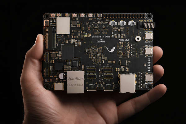
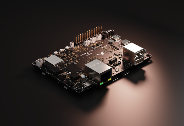
The Shrike Lite board by Vicharak is a unique hybrid development platform combining the RP2040 microcontroller with a Renesas Forge FPGA (1120 LUTs) on a single low-cost board. This makes it ideal for projects that mix software control with hardware-level timing precision, such as driving addressable WS2812 LED strips (a.k.a NeoPixels).
This blog walks through a real example from the official Shrike repository: the WS2812 example in the /examples/ws2812 folder. You’ll understand how the FPGA and microcontroller collaborate to send precisely timed LED data, why the FPGA is a great fit for high-speed protocols, and how the core Verilog logic interacts with the world.
What Are WS2812 LEDs and Why Do They Matter?
Before we dig into code and hardware architecture, let’s understand the physical device you’re driving.
WS2812 LEDs (often marketed as “NeoPixels”) are individually addressable RGB LEDs. Each LED package contains:
- Red, Green, and Blue LED elements.
- An integrated control chip that interprets incoming data.
- A single-wire data input and serial data output chain.
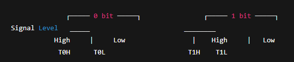
Key property: They use a single-wire, timing-sensitive protocol where the duration of high and low pulses determines whether a binary ‘0’ or ‘1’ is being transmitted.
WS2812 Single-Wire Data Protocol (Timing Essentials)
To understand what your FPGA needs to generate, here’s a simplified (yet accurate) timing breakdown based on typical WS2812 specifications:
| Bit | High time | Low time | Meaning |
|---|---|---|---|
| ‘0’ | ~300–500 ns | ~800 ns | Logical zero |
| ‘1’ | ~700–900 ns | ~450 ns | Logical one |
| Reset/Latch | > ~50 µs | — | Latches data into LEDs |
Each pixel needs 24 bits of data (8 bits per color: G, R, B). These bits are sent in GRB order.
This protocol has no clock line timing is embedded in the waveform itself. This is why microcontrollers often struggle: any jitter can corrupt the signal. FPGAs, with their deterministic hardware logic, are therefore a natural fit.
Shrike Lite Architecture Overview
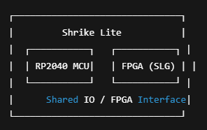
- RP2040 microcontroller handles configuration, communication, and high-level logic.
- FPGA handles precise timing and bit generation required by WS2812 data protocol.
- The two parts communicate through a shared interface to coordinate when and how data is sent.
The WS2812 Example: What’s Inside
The official WS2812 example inside the Shrike repo (under /examples/ws2812) includes:
Verilog FPGA logic (.v or .sv) — responsible for generating WS2812-compliant bit patterns.
C/C++ firmware for RP2040 — prepares color data and triggers the FPGA logic.
Makefiles / build scripts — to compile FPGA bitstream and RP2040 firmware.
Note: The precise file names and the entire code are in the GitHub repository you can explore them for complete implementation details.
Wiring and Circuit Diagram
Here’s a simplified connection diagram:
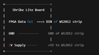
Important: WS2812 strips typically run at 5 V. Ensure shared ground and proper level shifting if driving from 3.3 V logic!
FPGA Logic: Timing Generation at Hardware Speed
Let’s break down the FPGA implementation conceptually.
Goals of FPGA Logic
- Accept a buffer of color values (24 bits × number of LEDs).
- Serialize these bits with precise timing.
- Drive the output pin to generate WS2812 pulse shapes within nanosecond accuracy.
How It Works
The FPGA implements a state machine that cycles through:
✔ Load next bit to transmit
✔ Drive output high for T0H or T1H depending on bit value
✔ Drive output low for the rest of the bit period
✔ Move to next bit or latch state
This is done in hardware, meaning each transition happens after deterministically defined clock cycles in the FPGA, eliminating jitter typical of software bit-banging. This degree of control is extremely hard to achieve on bare microcontrollers for hundreds of kilobits per second data rates.
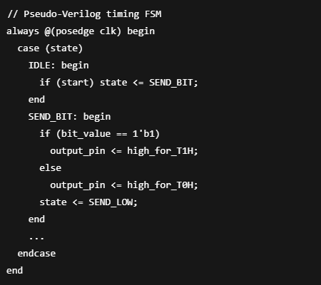
The actual code is in the examples/ws2812 folder, exploring it will make you comfortable with Verilog state machines and timing constraints.
RP2040 Firmware: Preparing and Triggering Data
Prerequisites
✔ Shrike Lite board
✔ WS2812 LED strip
✔ FPGA toolchain installed (Renesas/configure tools)
✔ RP2040 toolchain (e.g., Pico SDK + CMake)
Build Flow
- Compile FPGA bitstream from Verilog (Shrike tools)
- Compile RP2040 firmware
- Flash board with both FPGA + MCU code
- Supply power and observe LEDs
When triggered, the FPGA logic will send the first 24 bits for LED1, then for LED2, and so on — finally pulsing the line low for > 50 µs to latch and display the colors.
Wrap-Up: Hardwired Timing ≠ Software Loop
This example highlights the true strength of FPGAs:
When timing is everything, hardware beats software.
FPGA logic guarantees nanosecond-level timing without jitter, something microcontrollers cannot do reliably while running other tasks.
Shrike Lite’s hybrid architecture lets you balance both — use the RP2040 where flexibility is needed and the FPGA where precision is needed.
Suggested Next Steps
If this example intrigued you, try expanding it:
🔹 Add animations, update LED colors in real time
🔹 Chain more LEDs and optimize timing for large strips
🔹 Implement RGB patterns triggered via USB or serial
References