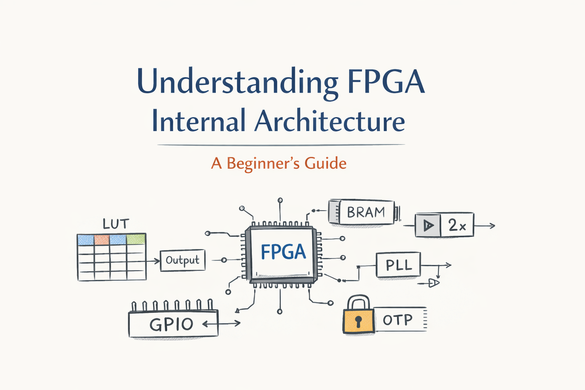
Understanding FPGA Internal Architecture : With Shrike

When people first hear the word FPGA, it often sounds intimidating—something abstract, complex, and very different from CPUs or microcontrollers. In reality, an FPGA is built from a small number of simple digital blocks, repeated many times and connected together in a programmable way.
In this log , we’ll explore the internal architecture of an FPGA, explaining what each block does and why it exists. To keep things concrete, we’ll use the Renesas Forge FPGA (SLG47910) found on the Shrike/Shrike-lite development board as a real, silicon-backed example.
Before we begin let me tell you what this blog is not about. This blog is not about :
- How to program the Shrike FPGA
- How to run your design on Shrike FPGA
- Or anything related to running anything on Shrike Dev board.
This is a dive into the internal of the FPGA on Shrike Dev kit or any FPGA in general.
Look-Up Tables (LUTs): The logic
At the heart of every FPGA lies a deceptively simple idea: instead of building logic from fixed gates, store the answers in memory. This idea is implemented using Look-Up Tables, or LUTs.
A LUT is not a gate. It is not an adder. It is not a comparator.
A LUT is a small memory that stores the output of a logic function for every possible input combination.
Why LUTs Exist in the First Place
To understand LUTs, it helps to first understand the problem they solve.
If an FPGA were built using fixed logic gates, the manufacturer would have to decide in advance which gates you might need and how they should be connected. That would make the chip inflexible. LUTs avoid this problem entirely.
Instead of hardwiring logic, the FPGA provides:
- A small memory (the LUT)
- A programmable interconnect
- Configuration bits that define behavior
This allows the same silicon to behave like any digital circuit, simply by changing what is stored in memory.
In other words:
An FPGA is programmable because its logic is stored, not wired.
What a LUT Really Is (Internally)
A LUT with N inputs is essentially a memory with 2ᴺ entries, each entry storing one bit.
For example:
- A 2-input LUT stores 4 bits
- A 3-input LUT stores 8 bits
- A 5-input LUT stores 32 bits
Each possible input combination selects one memory entry, and that entry becomes the output.
So when you write something like:
assign y = (a & b) | c;
The FPGA does not build an AND gate and an OR gate.
Instead, it computes the truth table for this expression and stores the results inside a LUT.At runtime, the LUT simply looks up the correct output.
LUTs in the Renesas Forge FPGA
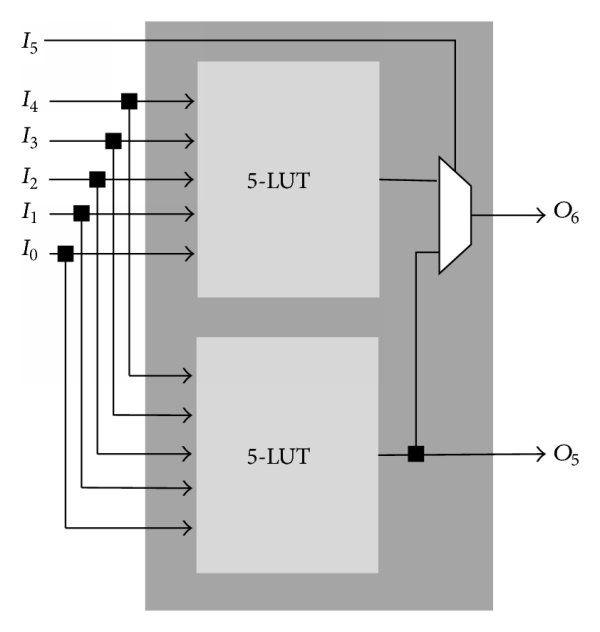
In the SLG47910 Forge FPGA, the fundamental logic element is a 5-input LUT (LUT5). That means each LUT can implement any Boolean function of up to five inputs.
Internally:
- Two LUT5s can be combined to form a 6-input LUT
- Each LUT output can optionally feed a flip-flop
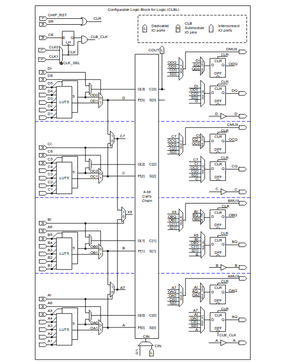
- LUTs are grouped into larger structures called Configurable Logic Blocks (CLBs)
Across the device, there are:
- 1120 LUT5, or equivalently
- 560 effective LUT6
This size is very well matched to control logic, finite state machines, protocol handling, and moderate arithmetic.
LUTs Are Physically Implemented
Although we talk about LUTs as “tables”, they are not implemented like SRAM arrays. Internally, LUTs are built using multiplexers.
Conceptually:
- Each input bit selects between two paths
- Multiple layers of multiplexers funnel down to one output
- The configuration bits determine which paths are selected
This multiplexer-based structure is one reason LUT-based FPGAs scale well and remain fast even when heavily reconfigured.
For beginners, the important takeaway is this:
A LUT is a programmable decision tree, controlled by configuration memory.
LUTs vs Logic Gates
One of the hardest mental transitions for beginners is letting go of gate-level thinking.
In FPGA design:
- You do not design gates
- You design behavior
- The FPGA figures out how to map that behavior into LUTs
This is why two very different-looking RTL descriptions can result in the same LUT usage after synthesis. The synthesis tool only cares about the truth table, not how you wrote the expression.
This also explains why:
- Complex Boolean expressions may fit into a single LUT
- Small changes in logic can dramatically change LUT usage
- Writing “clever” gate-level code rarely helps in FPGAs
LUTs and Arithmetic Logic
You might wonder how arithmetic like addition works if everything is just LUTs.
The answer is: LUTs implement the bit-level logic, and dedicated carry chains handle fast propagation of carry signals.
In the Forge FPGA:
- LUTs implement sum and control logic
- Built-in carry chains connect LUTs vertically
- This enables efficient adders, counters, and comparators
This hybrid approach keeps arithmetic fast while preserving flexibility.
LUTs as More Than Logic
One powerful aspect of LUTs is that they are not limited to logic functions.
In the Forge FPGA, LUTs can also be configured as:
- Small RAM blocks
- Shift registers
- Delay elements
When used this way, the LUT stops acting like a truth table and starts acting like storage. This dual-purpose nature is one of the reasons FPGAs are so versatile.
For beginners, this reinforces an important idea:
In an FPGA, logic and memory are closely related.
A Practical Beginner Insight
When you write RTL, you never explicitly say:
“Use a LUT here.”
But every combinational assign, every case statement, and every Boolean expression eventually becomes LUT contents.
So a good beginner mindset is:
- Write clear, readable RTL
- Let the synthesis tool worry about LUT mapping
- Learn to read utilization reports to see how logic maps onto LUTs
Once you understand LUTs, FPGA utilization reports stop being mysterious and start telling a story about your design.
D Flip-Flops (DFFs): Giving Logic Memory and Time
Pure logic is not enough to build useful systems. Digital designs need state—the ability to remember values across clock cycles. This is where D Flip-Flops, or DFFs, come in.
A D flip-flop stores a single bit of data and updates its output only on a clock edge. By combining many flip-flops, we can build registers, counters, pipelines, and finite state machines. In other words, flip-flops turn raw logic into synchronous systems.
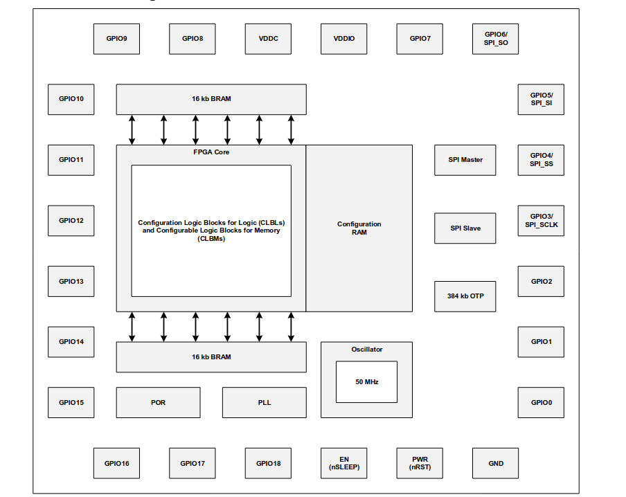
In the Forge FPGA, each LUT output has an associated flip-flop. This close pairing is intentional: it allows any combinational result to be registered immediately, which greatly simplifies timing closure. The SLG47910 contains 1120 D flip-flops, matching the number of LUTs one-to-one.
For beginners, this pairing is important to understand. When you write always @(posedge clk) in RTL, you are directly asking the FPGA to use these DFFs. LUTs compute values; DFFs store them and synchronize them to the clock.
Distributed SRAM: Memory Built from Logic
Beyond simple registers, many designs need small memories—for example, shift registers, FIFOs, or lookup tables. Instead of forcing designers to use large memory blocks for everything, FPGAs allow parts of the logic fabric itself to behave like memory. This is known as distributed SRAM.
In the Forge FPGA, certain configurable logic blocks can operate in special memory modes. When configured this way, LUTs no longer implement logic equations; instead, they store bits of data that can be read and written synchronously. The SLG47910 provides approximately 5 KB of distributed SRAM in total.
Distributed memory has some clear advantages. It sits very close to the logic that uses it, resulting in low latency and flexible placement. However, it is limited in size and not as power-efficient as dedicated memory blocks.
For beginners, the takeaway is simple: small memories are often built out of LUTs, while larger memories use dedicated blocks.
Block RAM (BRAM): Dedicated On-Chip Memory
For storing larger amounts of data, FPGAs include Block RAM, commonly called BRAM. Unlike distributed memory, BRAM is implemented as real SRAM macros on silicon. These blocks are faster, denser, and more power-efficient for bulk storage.
The Renesas Forge FPGA includes 32 KB of embedded Block RAM, split into two independent 16 KB BRAM blocks. Each block supports synchronous read and write operations and can be configured for different data widths and depths. Internally, these BRAM blocks are further divided into smaller slices, allowing flexible memory organization.
BRAM is typically used for things like buffers, tables, FIFOs, and small frame storage. Importantly, BRAM is not directly connected to GPIO pins; it is accessed only by the FPGA fabric itself.
From a learning standpoint, BRAM introduces the idea that not all memory in an FPGA is equal. Designers must choose between distributed memory and BRAM based on size, speed, and power requirements.
The way a BRAM interfaced depends from vendor to vendor the BRAM on Forge FPGA is bit different, it is interfaced over IO's where in some other vendors BRAM in available inside the FPGA core itself so the connections are taken care of router while mapping your design to FPGA.
On-Chip Oscillator (OSC): The Built-In Clock Source
All synchronous digital systems need a clock. While many designs use an external crystal or clock source, small FPGAs often include an internal oscillator to simplify system design.
The SLG47910 includes a 50 MHz on-chip oscillator. This oscillator can directly drive the FPGA core, the BRAM blocks, and even feed the PLL. Its presence allows the FPGA to operate without any external clock components, which is particularly useful for compact or low-cost designs.
For beginners, the oscillator represents convenience. It lets you focus on learning FPGA design without worrying about clock generation hardware. Later, as designs grow more complex, external clocks and clock conditioning become more important.
Phase-Locked Loop (PLL): Shaping and Controlling Clocks
While the oscillator provides a basic clock, many designs need clocks at different frequencies or with specific timing relationships. This is the role of the Phase-Locked Loop, or PLL.
A PLL can multiply or divide an input clock, reduce jitter, and generate multiple derived clocks. In the Forge FPGA, the PLL can take its input from either the internal oscillator or an external clock pin. Internally, the PLL supports very high frequencies, although practical logic speeds are limited by the rest of the device.
In beginner terms, the PLL is a clock transformer. You feed it one clock, configure a few parameters, and get a new clock that better suits your design. This is especially important for separating slow control logic from faster datapaths.
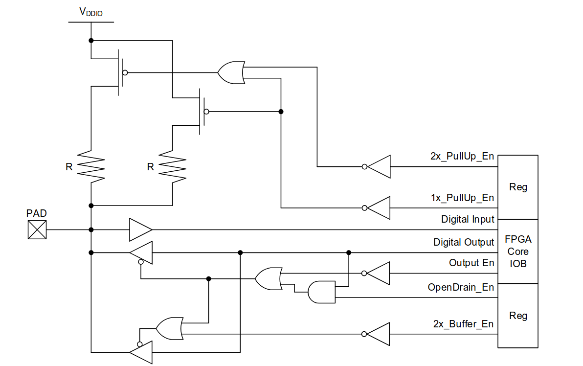
GPIO: Connecting the FPGA to the Outside World
An FPGA is useless if it cannot communicate with the outside world. This is the role of General-Purpose Input/Output (GPIO) pins.
The Forge FPGA provides 19 GPIO pins in the STQFN package used on the Shrike board. Each GPIO pin is highly configurable: it can act as an input, a push-pull output, or an open-drain output, with programmable drive strength and optional pull-up resistors. Internally, these pins connect to the FPGA fabric through IO Blocks (IOBs).
At first glance, GPIOs feel like the simplest part of an FPGA. In RTL, you write something like:
always @(posedge clk)
data <= gpio_in;
or
assign led = signal;
and it just works. This simplicity, however, hides a much more complex internal structure.
Why GPIOs Are Not “Just Wires”
A GPIO pin is not a direct wire from the FPGA fabric to the outside world. Instead, it passes through a dedicated circuit called an IO Block (IOB). This block exists because signals inside the FPGA and signals outside the chip live in very different electrical worlds.
Internally, FPGA logic operates at low voltage, low current, and controlled timing. Externally, GPIO pins must tolerate higher voltages, drive loads, protect against noise, and sometimes share buses with other devices. The IOB is what bridges this gap.
Internal Structure of a GPIO
Inside the Renesas Forge FPGA, each GPIO includes multiple sub-blocks working together:
- Input buffer
Converts the external voltage level into a clean digital signal that the FPGA fabric can safely use. - Output buffer
Drives the external pin with sufficient current and correct voltage levels. - Output Enable (OE) control
Determines whether the pin is actively driving or left in a high-impedance (Hi-Z) state. - Pull-up resistors
Optional weak resistors that pull the pin to logic high when nothing else is driving it. - Drive strength control
Allows selection between different output strengths (for example, 1× or 2× drive). - Open-drain support
Enables safe sharing of a signal line with other devices (common in I²C-style interfaces).
All of this logic exists even if you only write a single assignment in RTL.
Why This Complexity Is Necessary
Consider a simple output pin driving an LED. From RTL, it looks trivial. But electrically, the FPGA must decide:
- How much current to source or sink
- Whether the pin should default to Hi-Z during reset
- What happens if two devices accidentally drive the line
- How fast the signal edges should be to avoid ringing or EMI
The GPIO block handles all of this so that the FPGA fabric itself can remain clean, fast, and low power.
Bidirectional Pins and Tri-State Behavior
One of the most confusing concepts for beginners is bidirectional GPIOs. Internally, this is handled by separating the pin into three signals:
- Input signal → goes into the FPGA fabric
- Output signal → comes from the FPGA fabric
- Output Enable (OE) → controls whether the output buffer is active
When OE is disabled, the output buffer disconnects, and the pin becomes an input. This is why, in RTL, bidirectional pins are often described using separate in, out, and oe signals rather than a single inout.
Even though the Forge FPGA allows GPIO direction to be changed dynamically, the electrical mode (push-pull vs open-drain, pull-ups enabled, drive strength) is typically fixed at configuration time for safety and reliability.
Why Beginners Should Care
For someone learning FPGAs, it’s tempting to treat GPIOs as “simple pins.” But understanding their internal complexity helps explain:
- Why timing at IO boundaries matters
- Why drive strength and pull-ups exist
- Why some signals behave strangely during reset
- Why FPGA pin planning is important even for small designs
In short: GPIOs are where digital logic meets real physics.
A Helpful Mental Model
A good way to think about a GPIO pin is:
Inside the FPGA, it is a carefully controlled digital interface block.
Outside the FPGA, it is a raw electrical connection.
The GPIO block exists to make that boundary safe, flexible, and predictable.
OTP Block: Permanent Configuration Storage
One unique feature of the Forge FPGA family is its built-in One-Time Programmable (OTP) memory. OTP is a form of non-volatile memory that can be programmed exactly once and then permanently stores its contents.
The SLG47910 includes 384 KB of OTP memory, which is used to store the FPGA configuration bitstream. On power-up, the device automatically loads its configuration from this OTP, without needing any external flash or microcontroller.
This makes the FPGA behave much more like a traditional ASIC or microcontroller in production. It also provides strong security, since the configuration cannot be modified after programming.
From a beginner’s perspective, OTP explains how an FPGA can “remember” its design even when power is removed.
Bringing It All Together
Inside the Renesas Forge FPGA, every major building block has a clear role. LUTs compute logic, flip-flops store state, distributed SRAM and BRAM store data, clocking blocks control timing, GPIOs interface with the world, and OTP memory defines what the FPGA becomes at power-up.
Once you understand these pieces, you’ll find that nearly all FPGAs—large or small—follow the same architectural ideas. The Forge FPGA simply presents them in a compact, approachable form, making it an excellent learning platform.
Further Reading
This log is a comprehensive summary of the very basics of FPGA arch . There is a lot more to explore go checkout the datasheet in the references and also use the open internet to learn thing in depth.
Reference
https://www.renesas.com/en/document/dst/slg47910-datasheet?r=25546631
Courtesy
All the image and block diagram used are sourced from the renesas Forge FPGA datasheet.
https://www.renesas.com/en/document/dst/slg47910-datasheet?r=25546631
Cover image : Chat GPT 5.2